DOI:
https://doi.org/10.14483/23448393.23272Published:
2025-12-09Issue:
Vol. 30 No. 3 (2025): September-DecemberSection:
Electrical, Electronic and Telecommunications EngineeringExperimental Performance of a Two-Stage Cross-Coupled MOS-Based Circuit in the Solar and Piezoelectric Energy Harvesting
Análisis experimental del rendimiento de un circuito basado en MOS de par cruzado de dos etapas en la captación de energía solar y piezoeléctrica
Keywords:
piezoelectric energy, cross-coupled MOS, voltage multiplier, solar boost converter, solar energy harvesting (en).Keywords:
energía piezoeléctrica, MOS cross-coupled, multiplicador de voltaje, convertidor elevador solar, recolección de energía solar (es).Downloads
References
[1] M. Alibakhshikenari, V. B. Singh, C. H. See, R. A. A. Alhameed, F. Falcone, and E. Limiti,
“Energy harvesting circuit with high RF-to-DC conversion efficiency,” in Proc. IEEE Int. Symp. Antennas Propag. North Amer. Radio Sci. Meet., Montreal, QC, Canada, 2020, pp. 1299–1300. https://doi.org/10.1109/IEEECONF35879.2020.9329604
[2] N. Singh, “Low profile multiband rectenna for efficient energy harvesting at microwave frequencies,” Int. J. Elect., vol. 106, no. 12, pp. 2057–2071, 2019. https://doi.org/10.1080/00207217.2019.1636302
[3] U. Alvarado, A. Juanicorena, I. Adin, B. Sedano, I. Gutiérrez, and J. D. No, “Energy harvesting technologies for low-power electronics,” Trans. Emerg. Telecomm. Tech., vol. 23, no. 8, pp. 728–741, 2012. https://doi.org/10.1002/ett.2529
[4] M. D. Ker, S. L. Chen, and C. H. Tsai, “A new charge pump circuit dealing with gate-oxide reliability issue in low-voltage processes,” in Proc. IEEE Int. Symp. Circ. Syst. (ISCAS), Vancouver, BC, Canada, 2004, pp. 321–324.
[5] B. Jyostna and S. Murthy, “Low power CMOS start-up charge pump with power gating technique,” Int. J. Sci. Eng. Res., vol. 52, no. 4, pp. 1114–1118, 2016.
[6] W. Samakkhee, K. Phaebua, and T. Lertwiriyaprapa, “5.8 GHz rectifier circuit for electromagnetic energy harvesting system,” in Proc. Int. Symp. Ant. Propag. (ISAP2017), Phuket, Thailand, 2017, pp. 133–136. https://doi.org/10.1109/ISANP.2017.8229029
[7] F. Sari and Y. Uzun, “A comparative study: Voltage multipliers for RF energy harvesting system,” Comm. Fac. Sci. Univ. Ankara, vol. 61, no. 1, pp. 2–23, 2019. https://doi.org/10.33769/aupse.469183
[8] H. Goncalves, J. Fernandes, and M. Martins, “A study on MOSFET rectifiers maximum output voltage for RF power harvesting circuits,” in Proc. IEEE Int. Symp. Circ. Syst. (ISCAS), Lisbon, Portugal, 2013, pp. 2964–2967. https://doi.org/10.1109/ISCAS.2013.6572501
[9] Q. Li, J. Wang, D. Niu, and Y. Inoue, “A two-stage CMOS integrated highly efficient rectifier for vibration energy harvesting applications,” J. Int. Council Elect. Eng., vol. 4, no. 4, pp. 336–340, 2014. https://doi.org/10.1080/22348972.2014.11011893
[10] G. Chong et al., “CMOS cross-coupled differential-drive rectifier in subthreshold operation for ambient RF energy harvesting – Model and analysis,” IEEE Trans. Circ. Syst II Exp. Briefs, vol. 66, no. 12, pp. 1942–1946, 2019. https://doi.org/10.1109/TCSII.2019.2895659
[11] S. S. Chouhan and K. Halonen, “A modified cross coupled rectifier based charge pump for energy harvesting using RF to DC conversion,” in Proc. Eur. Conf. Circ. Theor. Des. (ECCTD), Dresden, Germany, 2013, pp. 1–4. https://doi.org/10.1109/ECCTD.2013.6662231
[12] S. Fan et al., “A cross-coupled active rectifier–booster regulator integrated circuit for broadband wireless energy harvesting system,” in MTT-S Int. Wireless Symp. (IWS), Shanghai, China, 2020, pp. 1–3. https://doi.org/10.1109/IWS49314.2020.9359959
[13] M. E. C. Andam, C. M. P. Canja, and M. A. Capilayan, “A design of self-biased cross coupled rectifier with integrated dual threshold voltage for RF energy harvesting application,” in Proc. 8th Int. Conf. Amb. Syst. Net. Tech., Madeira, Portugal, 2017, pp. 384–391.
[14] J. Banejee, “Comparison of cross couple MOS based and Schottky diode based RF energy harvesting circuits using Wilkinson power combiner,” Frequenz, vol. 77, pp. 133–146, 2023. https://doi.org/10.1515/freq-2022-0018
[15] M. W. Aljibory, H. T. Hashim, and W. N. Abbas, “A review of solar energy harvesting utilising a photovoltaic–thermoelectric integrated hybrid system,” Mater. Sci. Eng., vol. 1067, art. 012115, 2021. https://doi.org/10.1088/1757-899X/1067/1/012115
[16] L. Xiao, Y. S. Wu, and L. S. Yang, “Parametric study on thermoelectric conversion performance of a concentrated solar-driven thermionic-thermoelectric hybrid generator,” Int. J. Energy Res., vol. 42, pp. 656–672, 2018. https://doi.org/10.1002/er.3849
[17] D. Hao et al., “Solar energy harvesting technologies for PV self-powered applications: A comprehensive review,” Renew. Energy, vol. 188, pp. 678–697, 2022. https://doi.org/10.1016/j.renene.2022.02.066
[18] D. K. Sah, N. Mazumdar, P. Pal, and T. Amgoth, “A comprehensive study of solar energy harvesting system in wireless sensor networks,” in Proc. Int. Conf. Elect. Electron. Comp. Eng. (UPCON), Prayagraj, India, 2022, pp. 1–6. https://doi.org/10.1109/UPCON56432.2022.9986433
[19] N. Samal and O. J. Shiney, “Energy harvesting using piezoelectric transducers: A review,” J. Sci. Res., vol. 65, no. 3, pp. 3842–3847, 2021. https://doi.org/10.37398/JSR.2021.650320
[20] M. H. Amiri et al., “Piezoelectric energy harvesters: A critical assessment and a standardized reporting of power-producing vibrational harvesters,” Nano Energy, vol. 106, pp. 1–35, 2023. https://doi.org/10.1016/j.nanoen.2022.108073
[21] J. Ghazanfarian, M. Mohammadi, and K. Uchino, “Piezoelectric energy harvesting: A systematic review of reviews,” Actuators, vol. 10, no. 12, pp. 1–40, 2021. https://doi.org/10.3390/act10120312
[22] S. Dam and P. Mandal, “An integrated DC–DC boost converter having low-output ripple suitable for analog applications,” IEEE Trans. Power Electron., vol. 33, no. 6, pp. 5108–5117, 2018. https://doi.org/10.1109/TPEL.2017.2735491
[23] M. Maalandish, S. H. Hosseini, S. Ghasemzadeh, and E. Bab, “A novel multiphase high step-up DC/DC boost converter with lower losses on semiconductors,” IEEE J. Emer. Sel. Topics Power Electron., vol. 7, no. 1, pp. 541–554, 2019. https://doi.org/10.1109/JESTPE.2018.2830510
[24] L. Rodríguez, E. Raygada, C. Silva, and J. Saldaña, “Design of a CMOS cross-coupled voltage doubler,” in Proc. IEEE ANDESCON, Arequipa, Peru, 2016, pp. 1–4. https://doi.org/10.1109/ANDESCON.2016.7836258
[25] D. Kumar, P. Chaturvedi, and N. Jejurikar, “Piezoelectric energy harvester design and power conditioning,” in Proc. Conf. Elect. Electron. Comp. Sci., 2014, pp. 1–6. https://doi.org/10.1109/SCEECS.2014.6804491
[26] G. Revathi and R. Ingitham, “Piezoelectric energy harvesting system in mobiles with keypad and sound vibrations,” Int. J. Eng. Res. Tech. (IJERT), vol. 1, no. 4, pp. 1–4, 2012.
[27] M. H. Amiri et al., “Piezoelectric energy harvesters: A critical assessment and a standardized reporting of power-producing vibrational harvesters,” Nano Energy, vol. 106, pp. 1–12, 2023. https://doi.org/10.1016/j.nanoen.2022.108073
How to Cite
APA
ACM
ACS
ABNT
Chicago
Harvard
IEEE
MLA
Turabian
Vancouver
Download Citation
Recibido: 20 de febrero de 2025; Aceptado: 1 de septiembre de 2025
Abstract
Context:
Energy harvesting has positioned itself an emerging area of research due to recent developments in low-power electronics, the Internet of Things, and artificial intelligence. Various diode-based circuits and alternatives have been proposed in the literature, but the application of CMOS cross-coupled circuits, specifically in piezoelectric energy-harvesting systems, has not been properly explored.
Method:
An experimental study was conducted in order to assess the performance of a two-stage cross-couple MOS-based voltage multiplier in piezoelectric and solar energy harvesting. A piezoelectric disc was used to evaluate the output. The piezoelectric output was obtained by applying a small pressure to the input, and a 6 Vpanel was employed in the solar energy setup. Results: The proposed circuit provides a 1.91-fold voltage gain in the piezoelectric energy harvester.
Conclusions:
The two-stage MOS-based cross-coupled voltage multiplier circuit performs better than the diode-based alternative in the piezoelectric energy harvester. These experimental results show encouraging prospects for green energy, low-power electronics, and Internet of Things applications, among others.
Keywords:
piezoelectric energy, cross-coupled MOS, voltage multiplier, solar boost converter, solar energy harvesting.Resumen
Contexto:
La recolección de energía se ha posicionado como un área de investigación emergente debido a los desarrollos recientes en electrónica de baja potencia, el Internet de las Cosas y la inteligencia artificial. La literatura ha propuesto diversos circuitos basados en diodos y otras alternativas, pero la aplicación de circuitos CMOS de tipo cross-coupled, específicamente en sistemas piezoeléctricos de recolección de energía, no ha sido explorada adecuadamente.
Método:
Se llevó a cabo un estudio experimental para evaluar el desempeño de un multiplicador de voltaje de dos etapas basado en transistores MOS tipo cross-coupled en la recolección de energía piezoeléctrica y solar. Se utilizó un disco piezoeléctrico para evaluar la salida. La señal piezoeléctrica se obtuvo aplicando una pequeña presión en la entrada, y en la configuración solar se empleó un panel de 6 V.
Resultados:
El circuito propuesto proporciona una ganancia de voltaje de 1.91 veces en el recolector de energía piezoeléctrica. Conclusiones: El circuito multiplicador de voltaje de dos etapas, basado en transistores MOS tipo cross-coupled, presenta un mejor desempeño que la alternativa basada en diodos en el recolector de energía piezoeléctrica. Estos resultados experimentales brindan perspectivas alentadoras para aplicaciones de energía verde, electrónica de baja potencia y el Internet de las Cosas, entre otras.
Palabras clave:
energía piezoeléctrica, MOS cross-coupled, multiplicador de voltaje, convertidor elevador solar, recolección de energía solar.Introduction
Energy harvesting has positioned itself an emerging area of research due to recent developments in low-power electronics, the Internet of Things (IoT), and artificial intelligence (AI). Various diode-based circuits and alternatives have been proposed in the literature, aiming for the development of different technologies 1)(3.
For instance, 4 presented a review on powering different wireless sensors from ambient energy sources. Multiband RF energy-harvesting circuits 5 have also been proposed. 6 discussed the recent advancements in different energy-harvesting technologies, and 7 proposed the use of CMOS circuits for efficient RF-to-DC energy conversion. 8 used an NMOS RF-to-DC rectifier, achieving a 57.6% power efficiency. However, it is difficult to implement diode-based circuits in typical CMOS processes 9)(10). MOS-based energy harvesting circuits are rather scarce in the specialized literature, and they yield lower output voltage and power compared to conventional diode-based energy-harvesting circuits 11)(12). This is due to the large drain-to-source voltage drop 13.
MOS-based circuits (Dickson, Villard, etc.) offer better a performance. Among them, the Dickson charge pump is very popular in energy harvesting. For example, 9 proposed a high-gain MOS-based traditional Dickson charge pump circuit, and 10 introduced a step-up converter using a MOSFET-based Dickson charge pump. The latest development is a cross-couple MOS-based circuit 14)(15, which significantly improves AC-to-DC conversion efficiency while exhibiting a low ripple at the output when compared to MOS-based Dickson charge pumps. Furthermore, 16 proposed a modified cross-coupled energy-harvesting circuit that provided 46% efficiency using 180 nm CMOS technology. On the other hand, 17 proposed a cross-coupled active rectifier-booster for broadband wireless energy harvesting, and 18 proposed a self-bias cross-coupled MOS rectifier for RF energy harvesting. 19 compared the performance of diode-based and cross-coupled MOS-based circuits. However, to the best of the author’s knowledge, the application of CMOS cross-coupled circuits, specifically in piezoelectric energy-harvesting circuits, has not been properly explored in the literature. This work proposes a cross-coupled voltage multiplier circuit for solar 20)(23 and piezoelectric energy 24)(26 harvesting applications.
This study evaluated the experimental performance of a two-stage MOS-based cross-coupled voltage multiplier circuit for piezoelectric and solar energy-harvesting systems. 3205 n-channel and 9250 p-channel MOSFETs, as well as 100 nF capacitors, were used for designing the aforementioned circuit. The basic block diagram of this proposal is shown in Fig. 1. In addition, it should be noted that a self-driven solar-powered boost converter 27)(28 was considered.
Figure 1: Block diagram of the cross-coupled MOS-based piezoelectric energy-harvesting circuit
Cross-coupled MOS-based voltage multipliers and their advanta ges
Thetwo-stage cross-coupled MOS-based voltage multiplier circuit 29 is shown in Fig. 2. The circuit consists of two n-channel MOS and two p-channel MOS at every stage. It has a low threshold voltage drop andis suitable for energy-harvesting applications. The output voltage for the n-stage using Eq. (1).
Figure 2: Two-stage cross-coupled MOS-based energy-harvesting circuit
Experimental setup and performance análisis
A simple experimental setup was designed to analyze the performance of the proposed circuit. A 1 MHz function generator was used for applying the input voltage, as well as a dual trace CRO for observing the input and output waveform. The output voltage was measured by means of a voltmeter.
For the experimental study, a 1 V peak AC signal was applied at the input of the two-stage cross-coupled voltage multiplier circuit, which provided a 747 mV DC voltage at the output (Fig. 3).
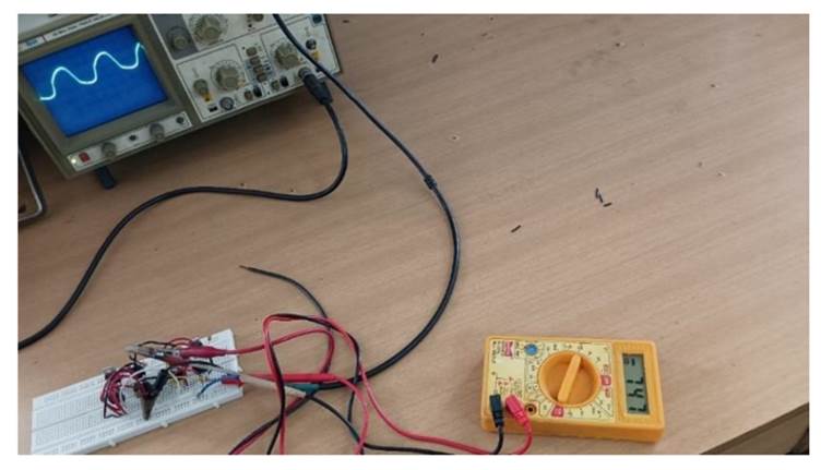
Figure 3: Rectified DC output voltage of the proposed circuit
Next, the performance of the multiplier circuit was studied in the context of a piezoelectric energy harvester, as shown in Fig. 4. Using one finger, a small pressure was applied on the disc-type piezoelectric materials. This yielded a 6.88 V rectified DC output voltage for a 3.6 V AC input.
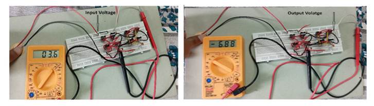
Figure 4: AC input and rectified DC output of the two-stage cross-coupled piezoelectric harvester
The output current of the Piezo-electric harvester was also measured. The maximum DC output current of the proposed multiplier circuit was 8 uA for a 1 KOhm load at the output (Fig. 5).
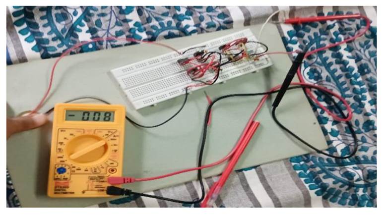
Figure 5: Output current of the proposed piezoelectric energy harvester
Then, we assessed the output performance of a three-stage Schottky diode-based voltage multiplier circuit in the piezoelectric energy harvester. This circuit is a combination of the Greinacher and Villard voltage multiplier circuits. At the input, a 2.5 V AC input signal was applied via piezoelectric pressure, as shown in Fig. 6. The analyzed circuit provided a 3.62 V rectified DC output voltage. This experimental study revealed that cross-coupled voltage multiplier circuits yield a comparatively higher output voltage than their diode-based counterparts in piezoelectric energy-harvesting circuits.
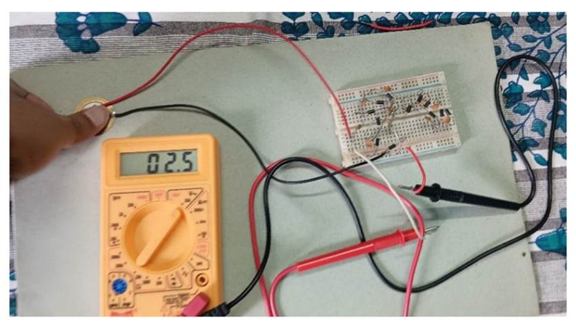
Figure 6: Input voltage from of the piezoelectric energy harvester with the diode-based circuit
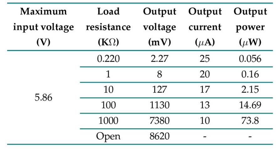
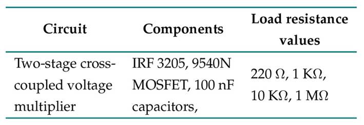
The different experimental output parameters of the piezoelectric energy harvester were determined for varying load resistance values. This is summarized in Table I.
Table I: Output parameters of the piezoelectric energy harvester for different load resistances
Afterwards, the performance of the cross-coupled voltage multiplier circuit was analyzed on a solar energy source. To this effect, a 6 V solar panel was used, with the aim of enhancing its output voltage. The DC output of the solar panel was converted into a pulse signal by means of a pulse generator, using a simple 7414 IC. The output voltage was 1.40, as well as 1.35 V for the open circuit, for a 1 MΩ resistance (Fig. 7).
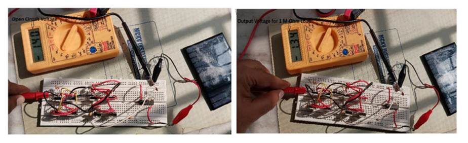
Figure 7: Voltages obtained for a 1 MΩ load resistance
The experimental results show that the cross-coupled voltage multiplier circuit provides a better output for the piezoelectric energy harvester when compared to the solar panel.
Comparison
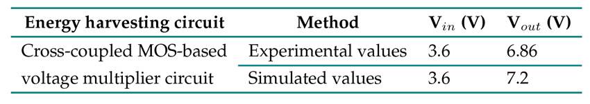
Using ORCAD 10.5, the simulated performance of the proposed cross-coupled voltage multiplier circuit was determined, as shown in Fig. 8. The results were compared against the findings from our experiments. The simulated vs. experimental output performance of the circuit in the piezoelectric energy harvester is shown in Fig. 9. Note that the experimental values almost follow the simulated ones. The same AC input voltage of 3.6 V was applied in both studies. As previously mentioned, 3205 n-channel and 9250 p-channel MOSFETs, as well as 100 nF capacitors, were used for designing the proposed circuit. Both MOS have a low resistance, and the 9250 p-channel exhibits a fast switching speed. On the other hand, the simulation employed a 3205 N MOSFET and 100 nF capacitors. The 3205 N MOSFET had a resistance of 8 mΩ. These MOSFETs can be operated at a 100 V drain-to-source voltage.
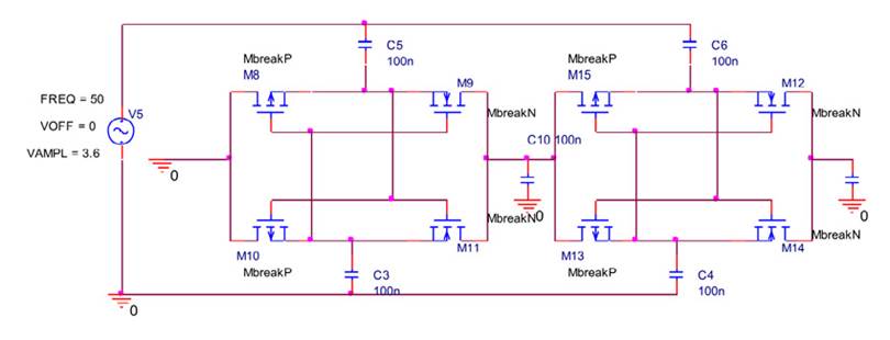
Figure 8: Two-stage cross-coupled MOS-based voltage multiplier circuit
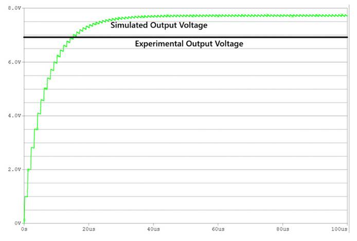
Figure 9: Comparison between experimental and simulated results
By means of simulation, a transient analysis of the proposed circuit was carried out.
The output power and the efficiency of the proposed circuit were also determined: it provides 2.2 mW of rectified output power for a 100 Ω load under a 1 V AC input (Fig. 10). The input power was calculated using Eq. (2).
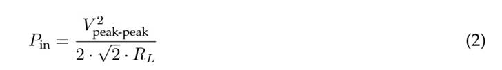
3.53 mWwereobtained for a 1 V AC input and a 100 Ω load resistance.
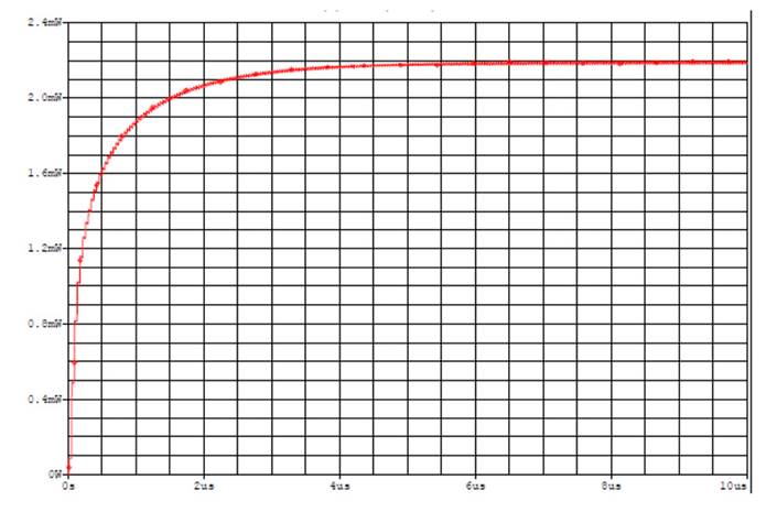
Figure 10: Simulated power for a 100 Ω load resistance
The proposed circuit exhibited a 62.32 % efficiency, as calculated using Eq. (3).

This experimental study revealed that our cross-coupled voltage multiplier is suitable for enhancing the output level of the analyzed piezoelectric energy harvester and solar-powered boost converter (Fig.11). Table II compares the output performance of different energy-harvesting sources.
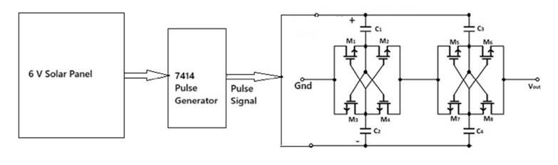
Figure 11: Solar-powered energy harvester
Table II: Comparison of experimental and simulated results for the proposed energy harvester
The design parameters of the proposed circuits are summarized in Table III.
Table III: Design parameters of the MOS-based cross-coupled circuit
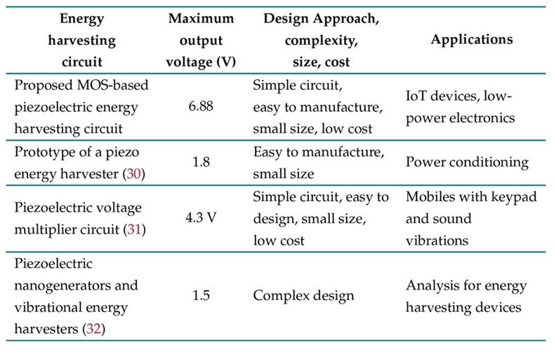
A comparison of the author’s proposed circuit against other energy-harvesting systems in the published literature is given in Table IV. This proposal shows significant improvements.
Table IV: Performance comparison vs. previously published energy-harvesting circuits
Conclusions
This work evaluated the experimental performance of a two-stage cross-coupled MOS-based voltage for piezoelectric and solar energy harvesting. The results show that the designed circuit performs better in piezoelectric energy harvesting, as it enhances the input voltage by 1.91 times.
A diode-based circuit was also evaluated in the piezoelectric energy harvester, providing a 1.44-fold increase in the output voltage compared to the input. The experimental study showed that the two-stage MOS-based cross-coupled voltage multiplier circuit performs better than the diode-based alternative, with encouraging prospects for green energy, low-power electronics, and IoT, among others.
References
License
Copyright (c) 2025 JOYDEEP BANERJEE

This work is licensed under a Creative Commons Attribution-NonCommercial-ShareAlike 4.0 International License.
![]()
From the edition of the V23N3 of year 2018 forward, the Creative Commons License "Attribution-Non-Commercial - No Derivative Works " is changed to the following:
Attribution - Non-Commercial - Share the same: this license allows others to distribute, remix, retouch, and create from your work in a non-commercial way, as long as they give you credit and license their new creations under the same conditions.

2.jpg)